All DataSheet
Home » Linear » LTC3895IFE DataSheet
LTC3895IFE DataSheet

LTC3895IFE DataSheet

Part No.
LTC3895IFE
Part Marking
LTC3895FE
Temperature
–40°C to 125°C
Package
38-Lead Plastic TSSOP
File Size
2385 KB
Page
38 Pages
Manufacturer
Linear Technology
Views
0
Upload Time
2022-08-01 11:46:48
Update Time
2022-08-01
Description
IC REG CTRLR BUCK 38TSSOP
If you would like to buy it now or in the future, please email or add our skype hello@ic-component.com

LTC3895IFE Features

■ Wide VIN Range: 4V to 140V (150V Abs Max)
■ Wide Output Voltage Range: 0.8V to 60V
■ Adjustable Gate Drive Level: 5V to 10V (OPTI-DRIVE)
■ Low Operating IQ: 40μA (Shutdown = 10μA)
■ 100% Duty Cycle Operation
■ No External Bootstrap Diode Required
■ Selectable Gate Drive UVLO Thresholds
■ Onboard LDO or External NMOS LDO for DRVCC
■ EXTVCC LDO Powers Drivers from VOUT
■ Phase-Lockable Frequency (75kHz to 850kHz)
■ Programmable Fixed Frequency (50kHz to 900kHz)
■ Selectable Continuous, Pulse-Skipping or Low Ripple Burst Mode® Operation at Light Loads
■ Adjustable Burst Clamp and Current Limit
■ Adjustable or Fixed (5V/3.3V) Output Voltage
■ Power Good Output Voltage Monitor
■ Programmable Input Overvoltage Lockout
■ 38-Lead TSSOP High Voltage Package

LTC3895IFE Applications

■ Automotive and Industrial Power Systems
■ High Voltage Battery Operated Systems
■ Telecommunications Power Systems

LTC3895IFE Description

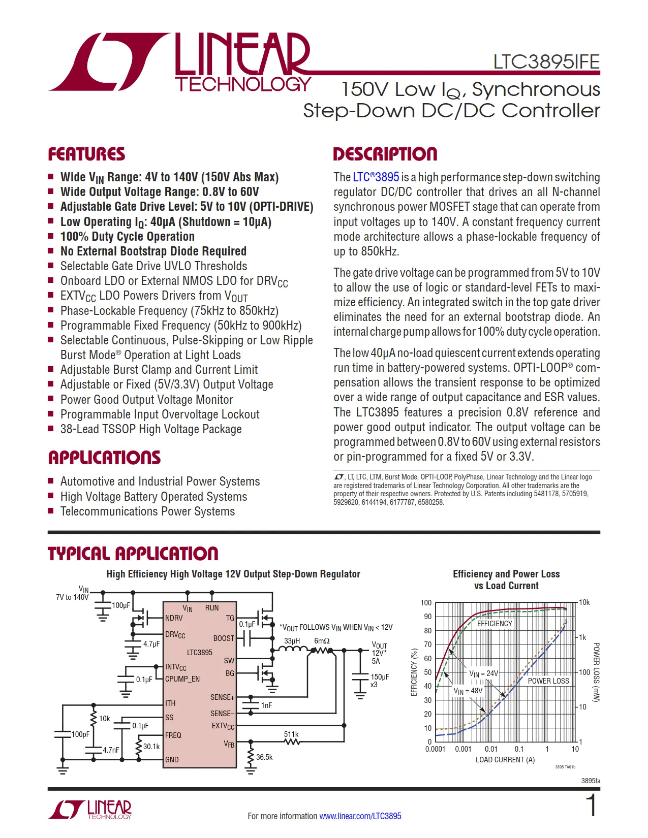
The LTC3895IFE is a high performance step-down switching regulator DC/DC controller that drives an all N-channel synchronous power MOSFET stage that can operate from input voltages up to 140V. A constant frequency current mode architecture allows a phase-lockable frequency of up to 850kHz.

The gate drive voltage can be programmed from 5V to 10V to allow the use of logic or standard-level FETs to maximize efficiency. An integrated switch in the top gate driver eliminates the need for an external bootstrap diode. An internal charge pump allows for 100% duty cycle operation.

The low 40μA no-load quiescent current extends operating run time in battery-powered systems. OPTI-LOOP® compensation allows the transient response to be optimized over a wide range of output capacitance and ESR values. The LTC3895IFE features a precision 0.8V reference and power good output indicator. The output voltage can be programmed between 0.8V to 60V using external resistors or pin-programmed for a fixed 5V or 3.3V.

Related LTC3895IFE Datasheet

Part No.
Datasheet

2385Kb / 38P

2385Kb / 38P

CopyRight © 2022 All DataSheet(www.all-datasheet.com)TXTLTADI