All DataSheet
Home » Linear » LT8609SIV DataSheet
LT8609SIV DataSheet

LT8609SIV DataSheet

Part No.
LT8609SIV
Part Marking
LGYN e4
Temperature
–40°C to 125°C
Package
LQFN (Laminate Package with QFN Footprint
File Size
1983 KB
Page
24 Pages
Manufacturer
Linear Technology
Views
2
Upload Time
2022-06-01 16:26:09
Update Time
2022-06-01
Description
42V, 2A/3A PEAK SYNC BUCK REG W/
If you would like to buy it now or in the future, please email or add our skype hello@ic-component.com

LT8609SIV Features

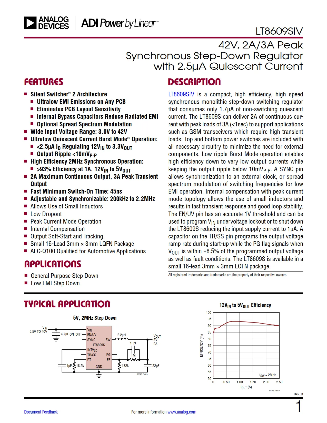
■ Silent Switcher® 2 Architecture
 □ Ultralow EMI Emissions on Any PCB
 □ Eliminates PCB Layout Sensitivity
 □ Internal Bypass Capacitors Reduce Radiated EMI
 □ Optional Spread Spectrum Modulation
■ Wide Input Voltage Range: 3.0V to 42V
■ Ultralow Quiescent Current Burst Mode® Operation:
 □ <2.5µA IQ Regulating 12VIN to 3.3VOUT
 □ Output Ripple <10mVP-P
■ High Efficiency 2MHz Synchronous Operation:
 □ >93% Efficiency at 1A, 12VIN to 5VOUT
■ 2A Maximum Continuous Output, 3A Peak Transient Output
■ Fast Minimum Switch-On Time: 45ns
■ Adjustable and Synchronizable: 200kHz to 2.2MHz
■ Allows Use of Small Inductors
■ Low Dropout
■ Peak Current Mode Operation
■ Internal Compensation
■ Output Soft-Start and Tracking
■ Small 16-Lead 3mm × 3mm LQFN Package
■ AEC-Q100 Qualified for Automotive Applications

LT8609SIV Applications

■ General Purpose Step Down
■ Low EMI Step Down

LT8609SIV Description

LT8609SIV is a compact, high efficiency, high speed synchronous monolithic step-down switching regulator that consumes only 1.7µA of non-switching quiescent current. The LT8609S can deliver 2A of continuous cur-rent with peak loads of 3A (<1sec) to support applications such as GSM transceivers which require high transient loads. Top and bottom power switches are included with all necessary circuitry to minimize the need for external components. Low ripple Burst Mode operation enables high efficiency down to very low output currents while keeping the output ripple below 10mVP-P. A SYNC pin allows synchronization to an external clock, or spread spectrum modulation of switching frequencies for low EMI operation. Internal compensation with peak current mode topology allows the use of small inductors and results in fast transient response and good loop stability.

The EN/UV pin has an accurate 1V threshold and can be used to program VIN undervoltage lockout or to shut down the LT8609S reducing the input supply current to 1µA. A capacitor on the TR/SS pin programs the output voltage ramp rate during start-up while the PG flag signals when VOUT is within ±8.5% of the programmed output voltage as well as fault conditions. The LT8609S is available in a small 16-lead 3mm × 3mm LQFN package.

Related LT8609SIV Datasheet

Part No.
Datasheet

1983Kb / 24P

CopyRight © 2022 All DataSheet(www.all-datasheet.com)TXTLTADI